
AMD K8L production capacity estimate
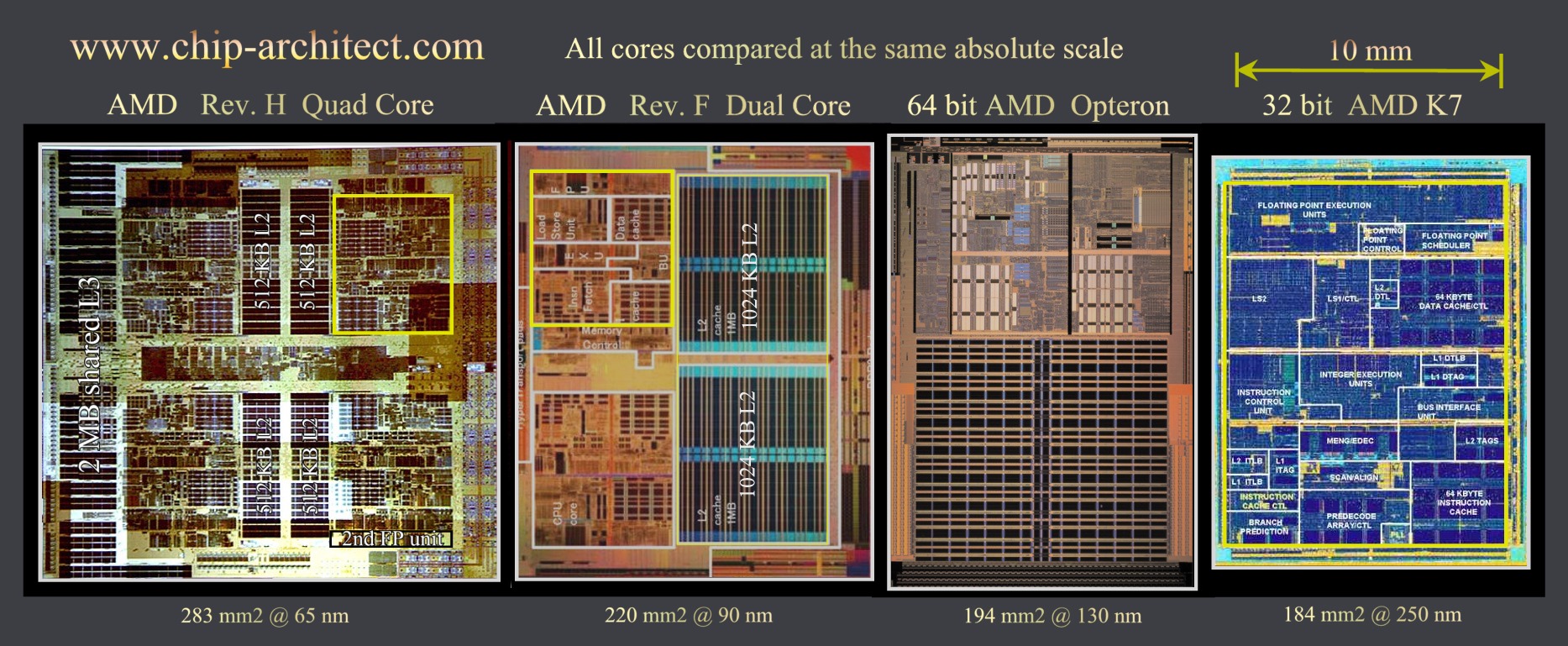
Look at this picture, which shows Rev H die size to be 283 mm^2.
Using a 17x18 geometry with the wafer program, we found a 300mm wafer can produce 202 dies. To take 100% of the server market, AMD needs to produce about 4 million K8Ls per quarter. In other words, it needs 20000 wafers per quarter, or 7000wspm. This leave 11000wspm to produce dual core desktop chips. We should expect Chartered to add at least 5000wspm.
posted by Sharikou, Ph. D. @ 10/13/2006 05:54:00 PM
![]()
![]()
42 Comments:
For a 'native' quad, that's pretty huge.
What about yield?
I am very suprised at the results.
Let me be the first to admit I am very suprised at the results, I always look at Sharikou's claims with a bit of uncertainty, but running the numbers, manufacturing capcity wise, AMD is in a strong position to gain market share from the beginning of 2008 and on.
2007 with all of the ramping and FAB conversions happening is the only reason I dont want to say from the middle of 2007, though looking at the numbers, they may very well gain market share.
First things first, I find the total number of server chips a little low, but well go with it, Sharikou is saying that there are only 16 Million server chips produced a year, out of the 230 Million chips expected to ba made in 2006, thats only 7% of all processors sold.
For 2007 well add about 10% growth, now where up to about 250 Million processors for 2007.
7% of 250 Million would be 17,710,000.
17,710,000 / 202 = 87,673 perfect wafers.
Lets assume AMD has 70% yield due to the complexity of the chip, leaving you with only 141 good Quad cores.
17,710,000 / 141 = 125,602 wafers, or 31,400 per quarter, or 10,466 wspm = 1,475,706 K8L's per month.
Now assuming that AMD gets to 15,000 wspm by the end of this year, and knowing that the 65nm conversion of FAB 30 will not be until the middle of 2007, is AMD going to use 70% of there 65nm manufacturing to cover a market that is only 7% of all processors made?
Oh yeah chartered, 5000 * 141 = 705,000, that would equal about 47% of the of the monthly total which would mean all AMD would have to do 5,466 wspm, equaling 36% of total FAB 36 capacity, at the beginning of 2007, not bad.
Now exiting 2007 is a different story, the number would only be 21% of total production, assuming 25,000 wspm at the end of the year.
But what does this do to 65nm dual core...
Assuming that die sizes for dual cores will be around 100mm you would get about 622 dual cores dies out of a 300mm wafer, now factor in yield and you have 435 dual cores dies.
435 * 9534 (wafers - the remaining 64% of production) = 4,147,293 dual cores processors per month, 4,147,293 * 3 (months) = 12,441,870 a quarter.
250 Million - 17,710,000 = 232,290,000 processors per year desktop and mobile, or 232,290,000 / 4 = 58,072,500 processors per quarter.
AMD having 12,441,870 of the 58,072,500 per quarter leaves them with 21% of the desktop and mobile, but at the same time having 100% of the server segment.
Also keep in mind that this is just FAB 36 and Chartered and 70% yield, FAB 30 has not been accounted for or the change in wspm to 25,000 by years end.
The numbers are very impressive, and I was suprised when I got done running them, it would seem AMD is poised to strike.
That's assuming AMD can get 100% yield, which IMO is unlikely. A 60% yield would be very good for such a large die. In this case the number should be adjusted to 33k wafters per quarter, or 12k wspm.
It would be good to AMD if it designed the quad core in such a way that if two cores have defect, they can be disabled without affecting the rest. Then the quad core can be sold as a dual core chip.
What about yield?
AMD's yield is about 2x of Intel's.
Another laughable false claim that is simply theoritically impossible..
You gave me a good laugh for a Friday Night.. Keep up the entertainment pretender...
Sharikou, Ph. D said...
What about yield?
AMD's yield is about 2x of Intel's.
I like the claim..
AMD's yield is about 2x of Intel's.
SO is AMD's profit...
" Sharikou, Ph. D said...
What about yield?
AMD's yield is about 2x of Intel's. "
Please elaborate.
-Longan-
"AMD's yield is about 2x of Intel's."
I guess if you say it enough people may actually start believing this?
Ummm, not sure about your "wafer program", but did you account for wafer edge exclusion and the scribe line area? I think # is actually <170 when you factor these in - unless AMD has one of tham magic saws when they dice up the wafers and runs a 0mm EE process....
Perhaps you can inform people of a typical scribe line area that is needed for dicing since you seem to know so much about capacity analysis and wafer programs? (Let me know if you need help with this)
And as others have mentioned may not want to be assuming 100% yield on that large a die, especially with such a large chunk of the chip being logic portions....
' "What about yield?
AMD's yield is about 2x of Intel's.'
Funny the question was how does yield factor into your capacity analysis and your response is AMD's yield is 2X of Intel's... If you are calculating AMD's capacity for a given die size, it really doesn't matter what Intel's yield is.
So to answer the other person's question - Shari-kook is assuming 100% yield - one error among many in his capacity analysis.
I think that this discussion has no sense. AMD is going to produce 55 milion CPUs next year - quad,dual and single core. Based on this numbers - you can estimate yelds, wafer output and fab utilization.
Nobody knows how many cores you can get from wafer. It is dark side of the manufacturers. Despite of APM, copy-exact etc. whatever both companies don't say about percentage of good chips from the single wafer.
If we talk about production capacity it grows every year.
AMD was able to produce 35 milion CPUs in 2004, 44 milion this year. It will be 55 CPUs in 2007. By the end of 2008 they are going to have two fabs and thrd one in NY in development. They target 50% of the market in 2010-2012 and it is more realistic than other numbers.
Its clearly not true they could ever get 100% of the server market unless Intel was nuked. The most they could realistically aim for is 75%, before the sales VP gets carted off in a white coat. That would of course leave much more room for desktop and mobile chips.
It would be interesting to get a an opinion on whether deactivating the L3 and 3rd and 4th cores on a duff K8L you could default to a regular 65nm DC? That would help AMDs yield mucho gracias.
However, this business of ramping depends on the product continuing to be competitive once Intel is 100% Conroe (and derivatives) on the desktop. Here Intel having such a large cache size means AMD is in a strong position price/performance wise.
Lets pretend they intentionally played this card and let Intel take a false victory with Conrunt.
Yeah.. oh that's nice ...
I'd hardly call it 2x, but it's true. http://www.theinquirer.net/default.aspx?article=30832
AMD is expecting quads to be 20% by end of 2007. Seems a bit high to me.
http://www.digitimes.com/mobos/a20061002PR207.html
Sharikou - this 283mm2 die size makes you happy. Heck, that's the size of 2 Core @ Extremes stuck together - on 65 nm. When Intel moves to 45nm that will go down further.
Frankly, I'm surprised that it's so large for what is supposedly a quad core design from the ground up. I expected better of AMD.
Anonymous - the Inquirer link you provided is wafer starts. Unfortunately, wafer starts does not equal CPU yield. And the link does not actually provide a comparision to Intel who may also be running their factories above capacity...or below. But I'll give you this - at least you provided a link. Unlike Sharikou who yanked yet another one out of thin air with his claim of AMD's yield being 2x Intel's.
One other minor diescrepancy with the theory that AMD will take 100% of the server market with this stunning new calculation. Hmmmm...it's called customer demand. Let's see - 90% of the market is DP. Even with crappy netburst AMD was not able to dislodge Intel substantially in DP. I'd be interested to see how they fare with Woodcrest which has already taken 40% of the DP market in 3 months since launch.
Sharikou the pretender of a Piled High and deep..
I have to admit entertainment level is high. With the invetion of interent one can spew one's own dribble and let others watch your jerking..
Look at the recent topics
CPU causes fires when its the battery
Patty hates AMD
INTEL going BK,
AMD has 2x INTEL yields..
The funny thing is AMD has had a great run. It is easier to selectively select truths and extrapolate. But the pretender continues to make up things...
You really must have been abused when you were young and impressionable Sharikou. I feel for your abuse.
Yes, but to take 100% of market AMD needs a vastly superior chip. In 1P and 2P space they don't have that. So even if they could provide 100% of the market. The market isn't demanding 100% AMD so this analysis is pretty pointless... sort of like this blog.
AMD's yield is about 2x of Intel's.
Sharikou, you don't know this for a fact. MOre lies from the lying liar.
Sharikou - this 283mm2 die size makes you happy. Heck, that's the size of 2 Core @ Extremes stuck together - on 65 nm. When Intel moves to 45nm that will go down further.
Dude, the dual core Opteron (socket F) is 220mm^2, a native quadcore so advanced at 280mm^2 is a piece of genius work. Dual independent mem controllers supports DDR2, DDR3, FB-DIMM, 48 bit physical address, HT3.0...
It will frag Intel like a scumbug.
Sharikou:
Aside from all the other weak points signaled by my predecesors:
Where are the motherboards and chipsets to suport all those chips?
As far as I can recall, AMD is not in the mobo making business, and the ATi merger is not completed yet....
Oh, and by the way, could you please show the RELEVANT server benchmarks to prove that demand will be so strong?
Cheers
NOTE: Relevant server benchmarcs are not framerates in DoomIII and Half life 2, but rather Apache on Windows and Linux, Oracle on Windows and linux, sendmail, Exchange server, etc.
WTF?
"a native quadcore so advanced at 280mm^2 is a piece of genius work. Dual independent mem controllers supports DDR2, DDR3, FB-DIMM, 48 bit physical address, HT3.0...
It will frag Intel like a scumbug."
Can you provide conclusive evidence of this claim? I think NOT! Just like INTEL going BK and INTEL cpus causing laptop fires... NO evidence but pure fabrication. SO .. STFU!
Remember when the Core2 benchmarks were releaed at IDF with real working silicon what dribble were you wspewing? All there is for the native quadcore is a die photo. Trust me they will take another two steppings to figure out what it ain't working properly right now. There are some serious speed path and fuctional issues that have been identified in post silicon debug.
LOL
"Dude, the dual core Opteron (socket F) is 220mm^2, a native quadcore so advanced at 280mm^2 is a piece of genius work."
It's just so funny how you distort facts and jump to wrong conclusion:
***The Opteron size you are quoting is 90nm, The quad at 65nm***
So you should halve the opteron die size to account for technology node difference. Now you have a 280mm2 quad vs a ~110mm2 dual core - still think it's genius, genius?
Dude, the dual core Opteron (socket F) is 220mm^2, a native quadcore so advanced at 280mm^2 is a piece of genius work. Dual independent mem controllers supports DDR2, DDR3, FB-DIMM, 48 bit physical address, HT3.0...
Again a lie from the pretender. 220mm^2 is on 90nm, which is more like 110mm^2 on 65nm. Let's see, that extrapolates to 220mm^2 for quad on 65nm. Someone doesn't know his grade school math yet!
"Graham said...
Yes, but to take 100% of market AMD needs a vastly superior chip. In 1P and 2P space they don't have that."
I think Sharikou mentioned 100% market share of server segment in his original post.
:P still I doubt Intel would go gently into that good night, nor would we (as consumers want to).
As for improved 1/2P, I guess you missed the core changes in K8L (which will also be used in the dual cores as well).
Changes to the core include
higher IPCs, 128 bit FP/Load, improved branch prediction among others. Also having an L3 cache will improve performance in some benchmarks.
C2D wasn't a magic bullet by any means. It featured (you guessed it) pretty much the same things that the new cores will add.
"18Sharikou said...
Heck, that's the size of 2 Core @ Extremes stuck together - on 65 nm."
Are you sure? With 2x4MB L2 cache?
The K8L on 65nm has just 2MB L3 + 4x512MB cache = 4MB cache, which is as much as a single Core 2 Duo.
As we all know, AMD doesn't need big caches to address the FSB bottleneck, so the 4MB/die on the C2D is needed.
Now just check out the pics of the die. The combined 4MB cache (L2 and L3) of the K8L already takes up abt 1/2 of the entire quad core die. I seriously doubt 2 x Core 2 Duo dies with 8MB L2 cache in total could fit into that same exact size!
The K8L on 65nm has just 2MB L3 + 4x512MB cache = 4MB cache, which is as much as a single Core 2 Duo.
Come on. Core 2 Duo is just a beefed up Pentium 3, a primitive piece of crap. A K8L has two memory controllers, 4 HT 3.0 links, true 64 bit, true virtualization... all sorts of high-tech. Intel's stuff is just ...primitive.
"The combined 4MB cache (L2 and L3) of the K8L already takes up abt 1/2 of the entire quad core die. I seriously doubt 2 x Core 2 Duo dies with 8MB L2 cache in total could fit into that same exact size!"
You wouldn't doubt if you would take time to do a simple google query on C2D die size since actually
they do fit in the same space:
Intel Core2 Duo Die Size 143 mm² / 111 mm²
Smaller is for Allendale and 2M L2, bigger is Conroe with 4M L2. Double that and you have almost exactly the same size as K8L.
"Come on. Core 2 Duo is just a beefed up Pentium 3, a primitive piece of crap"
And that crap based is beating everything currently existing under the Sun in almost every position and benchmark. Even the newest and greatest from AMD. Does that mean K8 is inferior to P3 in 1P/2P setup?
Hmm...that primative piece of crap is doing a number on the K8 lately...and if I remember correctly the K8 has the OMC, HT, "true 64bit" whatever that means and it is still getting beat. The I/O advantage is definately in Amd's favor, but the IPC advantage belongs to Intel. All these upgrades to the I/O system i.e. 2 memory controllers and 3.0 HT will mean nothing to 1p-2p systems since the cpu becomes the bottle neck in the system. By the way, why are we even talking about this? The K8L is vaporware right??? Or is a product only vaporware when it's from Intel?
Come on. Core 2 Duo is just a beefed up Pentium 3, a primitive piece of crap
so, a primitive piece of crap FRAG AMD's current most advanced chip. So, you indirectly concluded AMD chip is worse than the piece of crap ... I cannot find the english word to describe that. :)
Note: I'm not shooting AMD here, I shoot Sharikou statement. I do think AMD CPU is good, just that not as good when compared to Intel's for the current generation.
"220mm^2 is on 90nm, which is more like 110mm^2 on 65nm. Let's see, that extrapolates to 220mm^2 for quad on 65nm. Someone doesn't know his grade school math yet!"
Grade school math? If you had advanced to college you would have noticed that the quad core has an extra 2MB L3 cache, which would account for 20%+ die area.
Sharikou said...
"Come on. Core 2 Duo is just a beefed up Pentium 3, a primitive piece of crap."
What does that tell you about K8, and if Intel didn't go the MHz route where they would be today?
K8 is succesful because of Intels mistake, or can you spin that?
"Intel's stuff is just ...primitive."
Again what does that tell you.
Something so primitive is kicking AMD's latest processor technolgies ass (desktop/mobile/and up to 2P), and AMD can't do anything for at least 6 months.
I am very curious for you or anyone here to answer this...
What happens if Rev H (K8L) can not deliver on the performance speculated?
Don't just say it will with blind faith, answer the question.
Really..
"come on. Core 2 Duo is just a beefed up Pentium 3, a primitive piece of crap."
Last I checked that primitive piece of crap beat the crap out of AMD's best...
what a piece of crap.. heah peretender!
Now just check out the pics of the die. The combined 4MB cache (L2 and L3) of the K8L already takes up abt 1/2 of the entire quad core die. I seriously doubt 2 x Core 2 Duo dies with 8MB L2 cache in total could fit into that same exact size!
As was said before Core 2 Duo on the 65nm node is 143mm2 for Conroe and 111mm2 for Allendale with 4Mb and 2Mb of cache respectively.
Clovertown will basically be 2x143mm2 which is 286mm2 total which is about the same as Barcelona's die size.
Intel's cache density is superior on a given process then AMD's hence why Intel likes to throw cache on it's products more so then AMD does, since for AMD it costs more die space. Not to mention that fact that since AMD's uArch doens't benefit from cache improvements as much due to having a IMC.
Also were not too far from Intel moving to the 45nm versions of these CPU's when Barcelona is released.
A 3MB 45nm Dual Core for Intel, will be about 75mm2, while the 6MB version will be about 102mm2.
It would be interesting to get a an opinion on whether deactivating the L3 and 3rd and 4th cores on a duff K8L you could default to a regular 65nm DC? That would help AMDs yield mucho gracias.
Well that will probably occur as AMD is planning Dual Core K8L's with 2MB of LV3 and 2x512KB of cache, codenamed Antares.
As well we are also going to get a regular Dual Core K8L with just the 2x512KB of LV2 codenamed Arcturus.
***The Opteron size you are quoting is 90nm, The quad at 65nm***
So you should halve the opteron die size to account for technology node difference. Now you have a 280mm2 quad vs a ~110mm2 dual core - still think it's genius, genius?
220mm^2 is on 90nm, which is more like 110mm^2 on 65nm. Let's see, that extrapolates to 220mm^2 for quad on 65nm. Someone doesn't know his grade school math yet!
Optical shrinks are rarely perfect, so a 65nm 2x1MB LV2 K8 processor is going to be around a 132mm2 due to not everything being shrunk perfectly. However the 2x512KB version would be 110mm2 on 65nm. This is for Rev.G mind you based on K8.
If Rev.H Dual Cores are going to have 2x512KB of cache, then I expect it to be about 120mm2. And that for Dual Core without the extended 2MB LV3.
Hoever that aside 283mm2 for a Native Quad Core at 65nm is right where we expect it to be for AMD's K8L/Rev.H Quad Core. When Intel moves to their native Quad Cores on 45nm, I expect theirs to be only ~200mm2 or so due to the new process.
"Grade school math? If you had advanced to college you would have noticed that the quad core has an extra 2MB L3 cache, which would account for 20%+ die area."
Look at the die picture in the blog - you're telling me the L3 cache is >20% of that die?!?
And Sharikou as always misrepresented the die size comparisons (by using different tech nodes) to back up his inept conlcusions... What is worse the previous anonymous poster ignoring the L3 cahce difference or Sharikou mixing 90nm and 65nm data?
are these numbers correct?
core2:
4mb - 300mil
2mb - 170mil
thus 2mb cache = 130mil,
thus 2 cores + ? = 40mil
----------------------------------
amd x2
2mb - 230mil
1mb - 150mil
thus 1mb cache = 80 mil
thus 2 cores + memory + ? = 70 mil
is the memory control that big? or am i missing something? is it the virtualization?
AMD's capacity on FAB 36 will not reach 15K wspm by year's end. The actual schedule is:
10 K - end of 2006
15 K - mid 2007
20 K - end of 2007
25 K - mid 2008
FAB 30 is not quite as easy to estimate. FAB 30 will begin ramping down 90nm between the second and third quarters of 2007. 90nm production will reach zero between the second and third quarters of 2008. This would put the mid point about halfway through the 4th quarter of 2007. Theoretically, this is when 300mm production would begin testing. It is not clear how quickly FAB 38 would then ramp. However, it seems reasonable to follow the same ramp schedule as FAB 36. Since FAB 30 is not supposed to lose capacity in the switch to FAB 38 this would mean that FAB 38 would have to be at about 1/3 capacity on 300mm 65nm production when 90nm production reaches zero between Q2 08 and Q3 08. This would mean that tool installation would have to begin roughly at the end of the 3rd quarter of 2007. This would put FAB 38 at about 12K wspm by end of 2008.
However, this would mean a very rapid increase in production for AMD since FAB 38 would be shifting from 90nm 200mm to 65nm 300mm and then beginning the 45nm transition. Essentially, FAB 38 has to take on the volume increases once FAB 36 tops out at mid year in 2008. It should also be noted that FAB 38 would finally be the pay off for AMD with APM. Basically, AMD could move production from one FAB to the other the same day rather than two months later as required by Copy Exact.
From what I've seen about the K8L design I would estimate that K8L would close about 75% of the current C2D Integer IPC gap and match C2D in terms of SSE. The server market is much less certain since Woodcrest is currently hindered by FBDIMM. It is also uncertain whether Intel can remain competitive in 2008 using the same chipset structure that it is using for dual core. Intel badly needs CSI but that doesn't appear likely until later in 2009. Considering that HT 3.0 is already ahead of CSI in several ways it is less clear if CSI could be competitive at all if an HT 4.0 standard is out by then.
AMD's biggest problem is the memory cell size of the cache. AMD badly needs to implement TTRAM for L1 and L2 cache. It needs to implement TTRAM for L3 but Z-RAM would be better if it is fast enough.
When you remember to factor in yields, don't forget that as die area goes up, yield goes down. I've shown the proof in previous threads- you can look it up if you like. Why? Because defects are a function of area- the larger the die, the more likely a die is impacted by a killer defect.
Also, don't forget to subtract out your edge die (for a large die, at least 15-20% off the top).
So ultimately, if you start with a 70% yield on a 220mm^2 die (X2 AM2) you are looking at roughly 62% yield for the 283mm^2 die (K8L). For the 143mm^2 die (Conroe with same defect density), yield jumps to 81%. None of those numbers include the edge die loss either. Summary for 15% edge die loss and defect density that generates 70% yield on AM2 size die (noting that edge die loss is applied prior to defect yield):
Conroe (143): 359/494dpw = 73%
K8 X2 AM2 (220): 192/321dpw= 60%
K8L (283): 131/250 dpw= 52%
Note that my estimate was at 250dpw, not 202, and methods were consistent for all die. Also note that if you double Intel's defect density as our host would have you believe, the numbers look like this:
Conroe (143): 273/494dpw = 55%
which is still higher than K8, and more dpw that X2 AM2. Which means more $/wafer.
And that, our dear host, is what I would consider an analysis. BTW, that 131 dpw means ~10.2k wspm required just for K8L, which according to Scientia is full capacity at end 2006, so not impossible- but unlikely to alleviate capacity constraints.
"is the memory control that big? or am i missing something? is it the virtualization?"
I think the transistor count you have (Toledo and Manchester cores) is S939 K8, which does not have virtualization.
see here
Also, I believe the Conroe with 2MB L2 is the same with its 4MB L2 version, just half the L2 were disabled (perhaps due to defect). Where did you get the 170mil transistor count?
for example:
http://www.tomshardware.com/2006/07/14/core2_duo_knocks_out_athlon_64/page4.html
and i think i saw some numbers where the virtualization decreased the trans. count (by like 1-3mil, increased die-size tho)
i am a little confused over the intel numbers tho..a 130 mil 2mb cache + 2 little 20 mil cores...
anyone can post a pic of the intel core?
More implications of the yield analysis above:
Conroe (143): 359/494dpw = 73%
K8 X2 AM2 (220): 192/321dpw= 60%
K8L (283): 131/250 dpw= 52%
... assuming double defect density at Intel...
Conroe (143): 273/494dpw = 55%
This means, that compared to X2, Intel is getting 87% or 42% (1/2 yield claim) more dpw than AMD- which is huge when calculating $/wafer.
Compared to K8L, and assuming 2 Conroes per Kentsfield, that would be 37% or 5% (1/2 yield claim) more dpw than AMD. At $999 for both, that is an additional $5-50k per wafer of revenue. For 10k wspm, that is an additional $50-500 million of revenue per month!!!
Still think that die size doesn't make a huge difference to the top line?
"for example:
http://www.tomshardware.com/2006/07/14/core2_duo_knocks_out_athlon_64/page4.html"
I don't think those numbers are accurate. AFAIK, E6300/E6400 has the same core as the higher models, just with 2MB cache disabled. Toms Hardware could have been talking about the effective transistor count; but then, I have no idea how they come up with that value scientifically.
Core 2 Duo die photo is available from Intel.
"and i think i saw some numbers where the virtualization decreased the trans. count (by like 1-3mil, increased die-size tho)"
The reduction of transistor count, if there is, isn't due to virtualization, but the new (rev.F) core design.
Back to your original question - is the memory controller that big? K8's memory controller takes about 15% of die area, and K8 has 64KB L1 cache, which probably took another 10% of die area. Also, I think K8's AMD64 implementation allows it to access a wider range of physical memory (40-bit vs. 36-bit), which means another 10% difference in transistor count of the addressing logic.
Post a Comment
<< Home